The question came up at work, is inferred RAM compatible across different FPGA vendors?
My immediate answer was "yes", but then is it? And if there is some common VHDL code for multiple vendors, does it allow different implementations covering both LUT RAM and Block RAM? This study is limited to two major vendors, Xilinx and Altera as I have those tools installed, so should be a good starting point at least.
- Altera Inferred RAM template
- Single Port RAM
- Simple Dual Port RAM
- True Dual Port RAM
- Conclusions
- References
Altera Inferred RAM template
library ieee;
  use ieee.std_logic_1164.all;

entity sp_ram_intel is
  generic(
    DATA_WIDTH : natural := 8;
    ADDR_WIDTH : natural := 6
  );
  port(
    clk  : in  std_logic;
    addr : in  natural range 0 to 2**ADDR_WIDTH - 1;
    data : in  std_logic_vector((DATA_WIDTH-1) downto 0);
    we   : in  std_logic := '1';
    q    : out std_logic_vector((DATA_WIDTH -1) downto 0)
  );
end entity;


architecture rtl of sp_ram_intel is

  -- Build a 2-D array type for the RAM
  subtype word_t is std_logic_vector((DATA_WIDTH-1) downto 0);
  type memory_t is array(2**ADDR_WIDTH-1 downto 0) of word_t;

  -- Declare the RAM signal.
  signal ram : memory_t;

  -- Register to hold the address
  signal addr_reg : natural range 0 to 2**ADDR_WIDTH-1;

  -- Intel/Altera
  attribute ramstyle : string;
  -- Cyclone V: "M10K", "MLAB", "logic"
  attribute ramstyle of ram : signal is "MLAB";

begin

  process(clk)
  begin
    if rising_edge(clk) then
      if we = '1' then
        ram(addr) <= data;
      end if;

      -- Register the address for reading
      addr_reg <= addr;
    end if;
  end process;

  q <= ram(addr_reg);

end architecture;
This is the Altera preferred template which delays the address before reading the memory. This means the data output is not registered as-is.
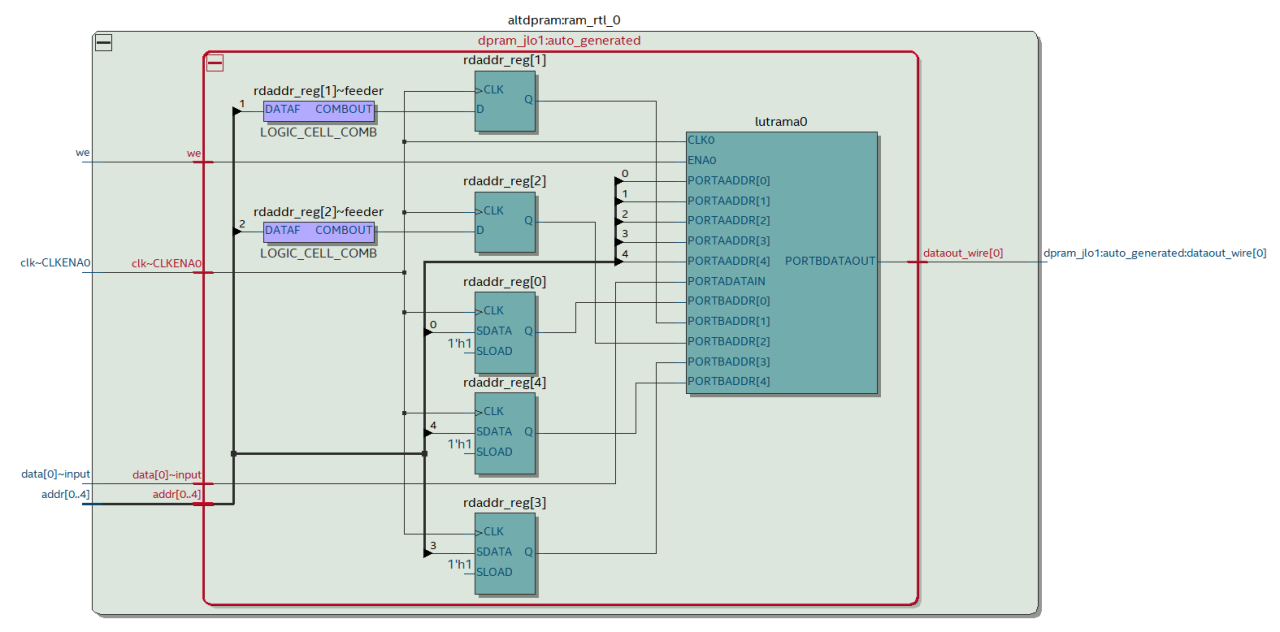
I prefer the Xilinx template because the outputs are registered. The Xilinx template also works just fine in Quartus Prime, see below. So I'll tidy up their code to be more VHDL-2008. Worth noting that ieee.numeric_std_unsigned does not appear to be available in Quartus Prime version 23.1, hence the long hand to make the code cross-vendor compatible.
Single Port RAM
library ieee;
  use ieee.std_logic_1164.all;

entity sp_ram is
  generic (
    addr_width_g      : integer := 10;
    data_width_g      : integer := 32;
    output_register_g : boolean := true;
    ram_style_g       : string  := ""
  );
  port (
    clk  : in  std_logic;
    we   : in  std_logic;
    ena  : in  std_logic;
    addr : in  std_logic_vector(addr_width_g-1 downto 0);
    din  : in  std_logic_vector(data_width_g-1 downto 0);
    dout : out std_logic_vector(data_width_g-1 downto 0)
  );
end entity;


library ieee;
  use ieee.numeric_std.all;

architecture common of sp_ram is

  type mem_array_t is array(integer range<>) of std_logic_vector(data_width_g-1 downto 0);

  signal ram      : mem_array_t(0 to 2**addr_width_g-1);
  signal ram_data : std_logic_vector(data_width_g-1 downto 0);

  attribute ramstyle  : string; -- Intel/Altera
  attribute ram_style : string; -- Xilinx

  attribute ramstyle  of ram : signal is ram_style_g;
  attribute ram_style of ram : signal is ram_style_g;

begin

  process(clk)
  begin
    if rising_edge(clk) then
      if ena = '1' then
        if we = '1' then
          ram(to_integer(unsigned(addr))) <= din;
        end if;
        ram_data <= ram(to_integer(unsigned(addr)));
      end if;
    end if;
  end process;

  output_register : if output_register_g generate
    --  Following code generates HIGH_PERFORMANCE (use output register)
    --  Following is a 2 clock cycle read latency with improved clock-to-out timing
    process(clk)
    begin
      if rising_edge(clk) then
        dout <= ram_data;
      end if;
    end process;

  else generate
    --  Following code generates LOW_LATENCY (no output register)
    --  Following is a 1 clock cycle read latency at the cost of a longer clock-to-out timing
    dout <= ram_data;
  end generate;

end architecture;
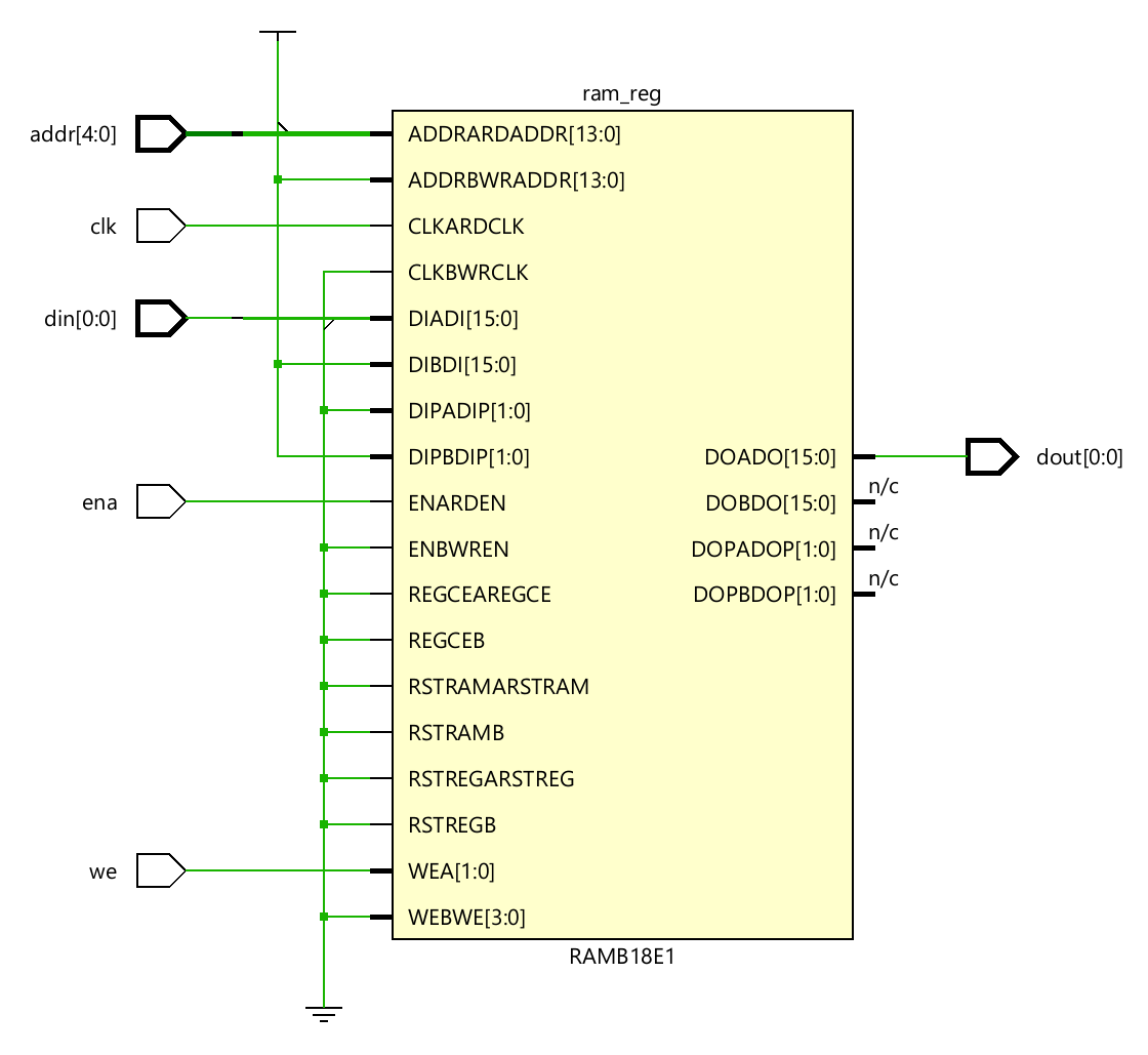
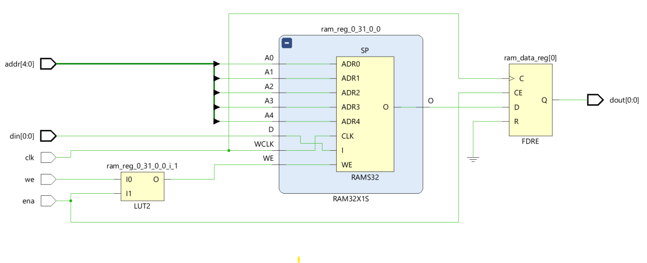
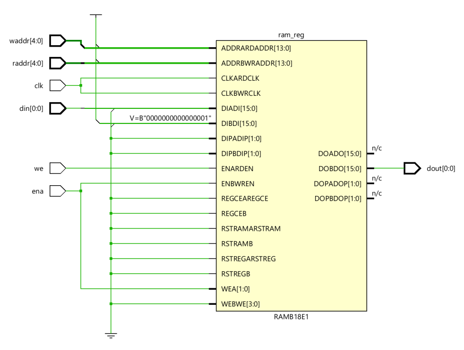
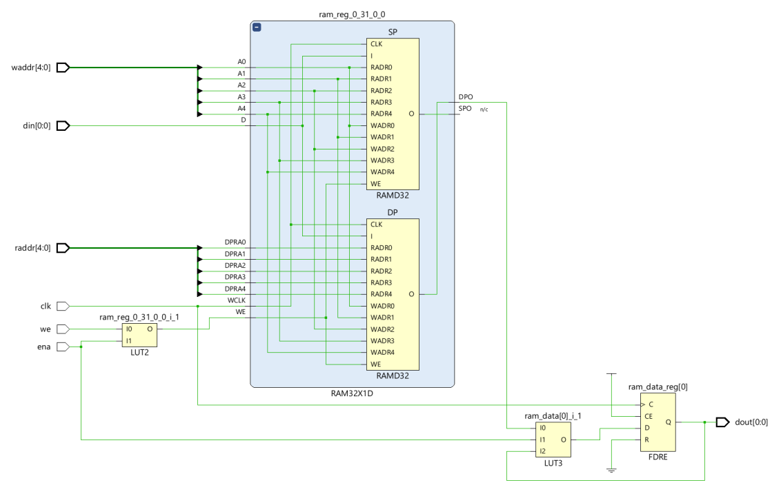
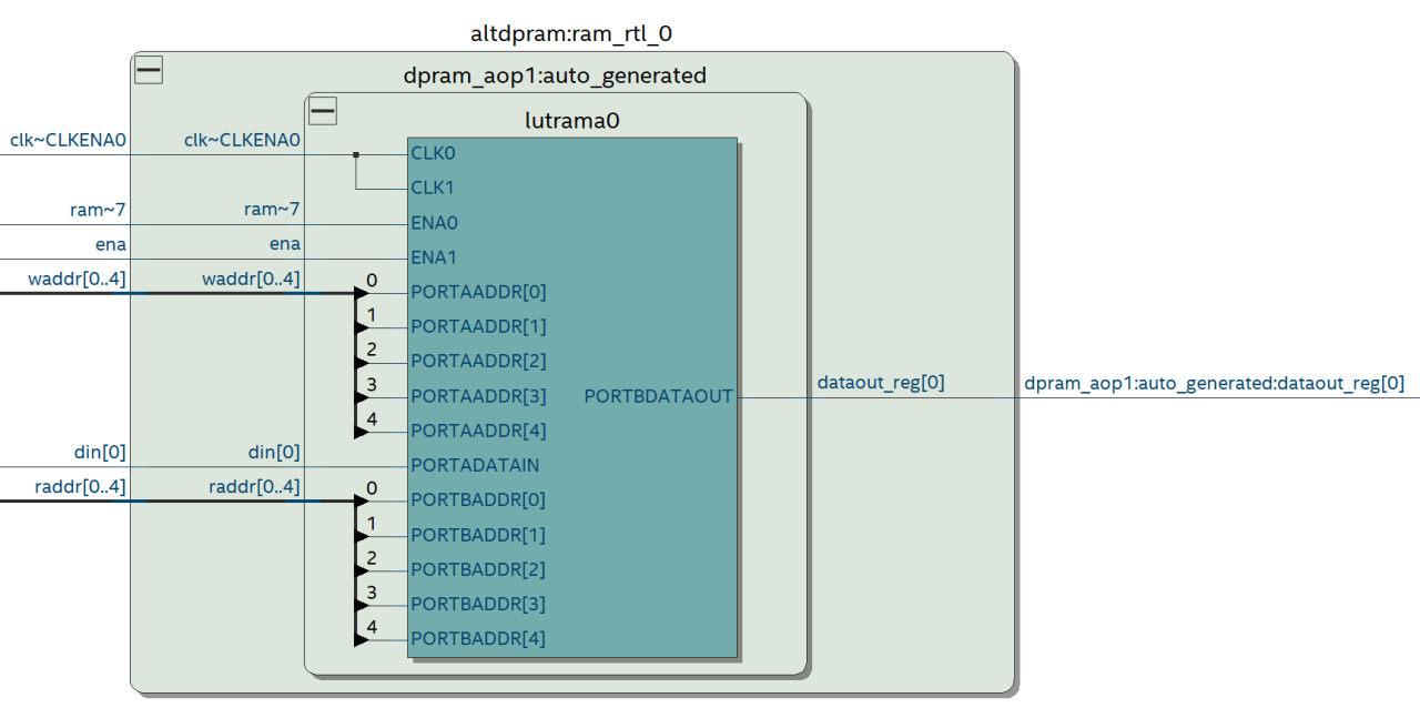
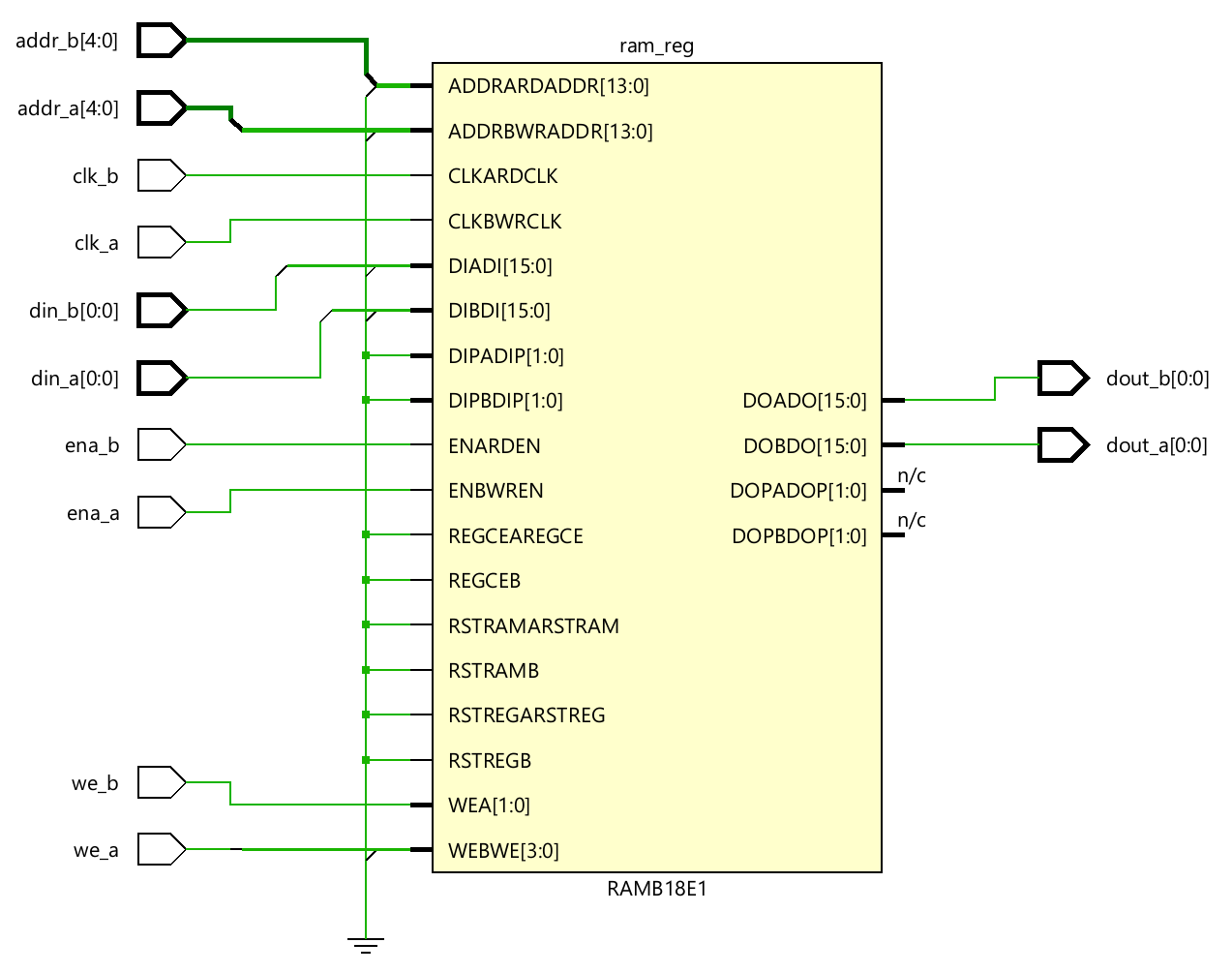
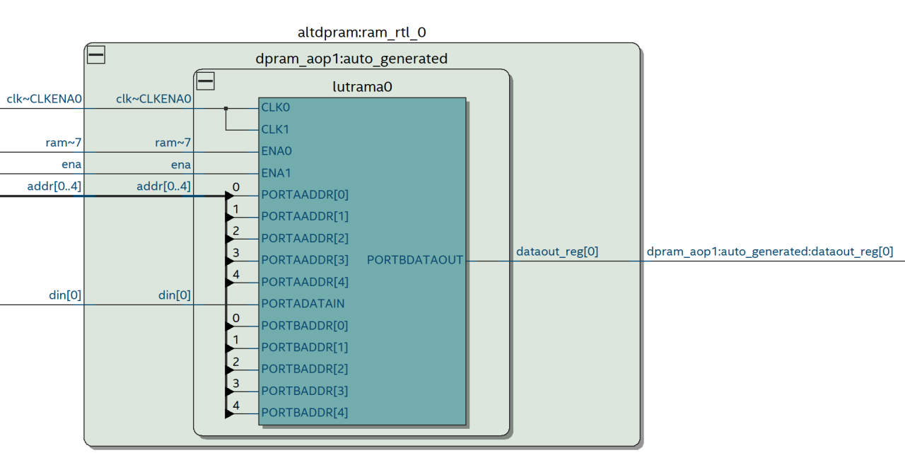
This template will infer both LUT RAM and Block RAM for both Vendors as the schematics show below.
Xilinx's automatic RAM implementation choice works based on a threshold of 1,024 bits of RAM. At or above 1,024 bits BlockRAM is preferred to distributed RAM. This has been verified by synthesis in the following results table and also by reducing the address width to 1.
| Data Width (bits) | |||||||||||||||
|---|---|---|---|---|---|---|---|---|---|---|---|---|---|---|---|
| 8 | 15 | 16 | 24 | 28 | 30 | 31 | 32 | 36 | 37 | 63 | 64 | 127 | 128 | ||
| Address Width (bits) | 3 | D: 64 | D: 120 | D: 128 | D: 192 | D: 224 | D: 240 | D: 248 | D: 256 | D: 288 | D: 296 | D: 504 | D: 512 | D: 1,016 | B: 1,024 |
| 4 | D: 128 | D: 240 | D: 256 | D: 384 | D: 448 | D: 480 | D: 496 | D: 512 | D: 576 | D: 592 | D: 1,008 | B: 1,024 | B: 2,032 | B: 2,048 | |
| 5 | D: 256 | D: 480 | D: 512 | D: 768 | D: 896 | D: 960 | D: 992 | B: 1,024 | B: 1,152 | B: 1,184 | B: 2,016 | B: 2,048 | B: 4,064 | B: 4,096 | |
| 6 | D: 512 | D: 960 | B: 1,024 | B: 1,536 | B: 1,792 | B: 1,920 | B: 1,984 | B: 2,048 | B: 2,304 | B: 2,368 | B: 4,032 | B: 4,096 | B: 8,128 | B: 8,192 | |
| 7 | B: 1,024 | B: 1,920 | B: 2,048 | B: 3,072 | B: 3,584 | B: 3,840 | B: 3,968 | B: 4,096 | B: 4,608 | B: 4,736 | B: 8,064 | B: 8,192 | B: 16,256 | B: 16,384 | |
| 8 | B: 2,048 | B: 3,840 | B: 4,096 | B: 6,144 | B: 7,168 | B: 7,680 | B: 7,936 | B: 8,192 | B: 9,216 | B: 9,472 | B: 16,128 | B: 16,384 | B: 32,512 | B: 32,768 | |
In the table above "D:" means the automatic implementation chose a distributed or LUT RAM, "B:" means the implementation was a block RAM. The cell values are the number of bits required for the given data and address bits, i.e. (2**addr_width_g) * data_width_g.
The choice can also be asserted by the developer through a custom VHDL attribute.
attribute ram_style : string; -- Xilinx
attribute ram_style of ram : signal is "distributed";

Getting LUT RAM to work with Altera devices is a manual process. There's a hint of an "auto" option in the explanation of the RAMSTYLE_ATTRIBUTE attribute, and the description of the Memory Block Types (relates to and older version 17 of Quartus Prime) but I did not find it worked. Despite these suggestions block RAM is the default implementation and MLAB (LUT RAM) can only be created by explicit request. One can either use an assignment in Quartus Prime or VHDL attribute to set the RAM style as follows.
set_instance_assignment -name RAMSTYLE_ATTRIBUTE MLAB -to ram
Use of this avoids the addition of custom VHDL attributes that are different between vendors. Although the addition of multiple attributes has not be an issue in the template code provided here.
"Any attribute not recognized by a particular tool is ignored."
The equivalent custom VHDL attributes for Altera are shown below.
attribute ramstyle : string; -- Intel/Altera
attribute ramstyle of ram : signal is "MLAB";
Simple Dual Port RAM
library ieee;
  use ieee.std_logic_1164.all;

entity sdp_ram is
  generic (
    addr_width_g      : integer := 10;
    data_width_g      : integer := 32;
    output_register_g : boolean := true;
    ram_style_g       : string  := ""
  );
  port (
    clk   : in  std_logic;
    we    : in  std_logic;
    ena   : in  std_logic;
    raddr : in  std_logic_vector(addr_width_g-1 downto 0);
    waddr : in  std_logic_vector(addr_width_g-1 downto 0);
    din   : in  std_logic_vector(data_width_g-1 downto 0);
    dout  : out std_logic_vector(data_width_g-1 downto 0)
  );
end entity;


library ieee;
  use ieee.numeric_std.all;

architecture common of sdp_ram is

  type mem_array_t is array(integer range<>) of std_logic_vector(data_width_g-1 downto 0);

  signal ram      : mem_array_t(0 to 2**addr_width_g-1);
  signal ram_data : std_logic_vector(data_width_g-1 downto 0);

  attribute ramstyle  : string; -- Intel/Altera
  attribute ram_style : string; -- Xilinx

  attribute ramstyle  of ram : signal is ram_style_g;
  attribute ram_style of ram : signal is ram_style_g;

begin

  process(clk)
  begin
    if rising_edge(clk) then
      if ena = '1' then
        if we = '1' then
          ram(to_integer(unsigned(waddr))) <= din;
        end if;
        ram_data <= ram(to_integer(unsigned(raddr)));
      end if;
    end if;
  end process;

  output_register : if output_register_g generate
    --  Following code generates HIGH_PERFORMANCE (use output register)
    --  Following is a 2 clock cycle read latency with improved clock-to-out timing
    process(clk)
    begin
      if rising_edge(clk) then
        dout <= ram_data;
      end if;
    end process;

  else generate
    --  Following code generates LOW_LATENCY (no output register)
    --  Following is a 1 clock cycle read latency at the cost of a longer clock-to-out timing
    dout <= ram_data;
  end generate;

end architecture;
Worth mentioning here the means to set the generics in each tool to allow for easy testing of the variations.
set_property generic {data_width_g=32 addr_width_g=8 output_register_g=false ram_style_g=\"distributed\"} [current_fileset]
set_parameter -name output_register_g true
set_parameter -name addr_width_g 5
set_parameter -name data_width_g 1
set_parameter -name ram_style_g "\"MLAB\""
True Dual Port RAM
A previous blog on RAM inferencing used and explained the Vivado true dual port RAM template and its shortcomings. Intel Quartus Prime Pro Edition User Guide provides a template for True Dual-Port Synchronous RAM but it for a single clock domain only. Oddly, Xilinx's Vivado template does work in Altra's Quartus Prime.
Note, I have not been able to infer true dual port RAM as LUT RAM, only block RAM, in both Vivado and Quartus Prime. This is perhaps to be expected. Also a Xilinx forum post "How to simulate inferred dual port dual clock block rams?" suggests a VHDL implementation with signals which I was unable to get working in Quartus Prime, but it did work in Vivado. So this version is not a compatible way to infer RAM even if it removed the VHDL-93 style shared variable usage.
Conclusions
The purpose of this blog was to provide proof by code and synthesis results that there is a common way to infer RAM from VHDL.
- There seems to be a template for inferring RAM that works with at least two FPGA vendors.
- The template works for both LUT (distributed) RAM and Block RAM unless its a true dual port inference.
- A generic can be used to pass in the required RAM style by using the union of all custom VHDL RAM style attributes without complaint.
