Low Speed Serial I/O Variable Delay Monitoring
I have previously had success with adjusting the IDELAY component to optimise the sample point for low speed serial I/O. I was getting the desired results, but I had little insight into the actual behaviour which I assumed was much as I had coded with no errors whatsoever. The functionality of this design is FPGA device specific and outside the realms of realistic simulation. That makes it a good candidate for the Internal Logic Analyser (ILA), not least because I have used the ILA so infrequently that it is not a skill I have developed and maintained.
- Process
- VHDL Attributes
- Synthesis
- Remainder
- Scripts
- Changing the IO Frequency
- Results
- Pass
- Fail
- Conclusions
- References
Process
Firstly I worked through the build process manually in project mode. Then I captured the process in a TCL build script in order to make it quicker and more repeatable for experimentation.
VHDL Attributes
In order to select nets that illustrated how the design was behaving, I originally tried using synthesis results. By the time the netlist has been synthesised too many signals names (nets and registers) appeared to have changed in order to right click and "Mark Debug". So I opted instead for the use of VHDL attributes.
Retaining Names of Debug Probe Nets Using MARK_DEBUG
You can mark a signal for debug either at the RTL stage or post-synthesis. The presence of the MARK_DEBUG attribute on the nets ensures that the nets are not replicated, retimed, removed, or otherwise optimized. You can apply the MARK_DEBUG attribute on top level ports, nets, hierarchical module ports and nets internal to hierarchical modules. This method is most likely to preserve HDL signal names post synthesis. Nets marked for debugging are shown in the Unassigned Debug Nets folder in the Debug window post synthesis.
Add the mark_debug attribute to HDL files as follows:
VHDL:
attribute mark_debug : string;
attribute mark_debug of <net> : signal is "true";
This method also preserved the enumerated types names too, e.g. FSM state names, when displaying the waveforms in the ILA wave viewer.
Synthesis
You will need to synthesise the VHDL with signals marked for debug, then "Set Up Debug" in order to include the ILA Debug cores that I have not manually instantiated in the VHDL code. Because of that lack of instantiation, this step is required every time you build. I set the "Sample of data depth" to 4096 which neatly covered the 31 IDELAY offsets I wanted to test.
Remainder
Then complete the build process to its logical conclusion using:
- Implementation
- Generate Bitstream
- Program Device
Scripts
The above is encapsulated in two TCL scripts. One to amend the I/O data frequency at which to run the test. The second to make the ILA build repeatable and slicker without manual mouse clicks.
Changing the IO Frequency
First amend the clock frequency specified for lssio_freq in ip_gen_idelay.tcl, then run the ila.tcl script to include the ILA debug core.
# Adjust:
# set lssio_freq xx.0
source {ip_gen_idelay.tcl}
# Run the above build process in project mode
source {ila.tcl}
Results
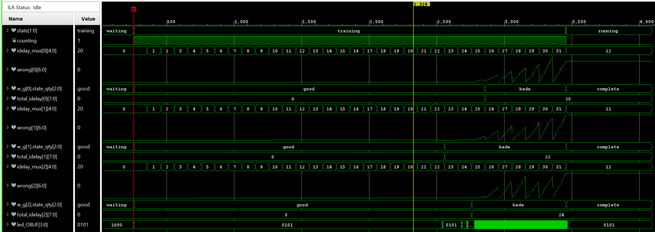
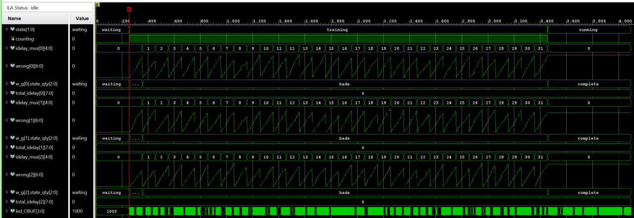
On this occaision, with slightly different environmental factors over the previous blog, I was passing at 108 MHz and failing at 109 MHz. These are the two ILA waveforms to show what is going on internally to the FPGA. Note it is not possible to tap the pad for debug, e.g. to see the "eye of the data", as the design will fail to route as a result of that probe point choice.
Pass

The waveform above shows the measurement at each IDELAY offset. When the measurement is non-zero, the offset is noted for each lane (25, 22, 24 respectively), and then halved for the eye of the data (12, 11, 12 respectively). Had there been any offset measurement error at the start of the sweep, the final value would be the average. The only effect of changing the input delay constraints was to bring the point at which errors were detected for the higher IDELAY delays to the left. I was unable to ramp up the errors on the left hand side. It is possible to change the range over which the sampling occurs by changing the phase of the clk_rx_pll created from the data receive clock, clk_rx. I experimented with a wide range of phase values and I did not get the commensurate shift in error detection I was expecting, which lead me re-examine my original design without identifying any obvious issues.
Fail

When the PRSB check failed, it failed across the boards of IDELAY offsets. i.e. It failed catastrophically between working and not working with 1 MHz difference.
Conclusions
The design was amended once the actual internal workings were made visible, in a way that had not been elucidated by simulation alone. The result was only mildly changed in a non-significant way. I have ignored the timing warnings for the external I/O where the wires feed from OBUF to IBUF with IDELAY, not least because only a large negative minimum input delay makes any difference to the results.
References
- Github Source Code
- Low Speed Serial I/O, Variable Phase Delay
- Vivado Design Suite Tutorial: Programming and Debugging, Xilinx UG936
2 comments
Comment from: philip Member
Comment from: philip Member
Xilinx would appear to have already written an IP core for their FPGAs according to this document: LDPC Encoder Decoder v1.0 Product Brief (PB052)
No! I’m afraid I had to look Low-density parity-check code up on Wikipedia. I will have to consider that, thanks for the pointer. I did find the 01 signal sampling was superior to these methods. BTW I am currently double checking my work here as it happens.